|
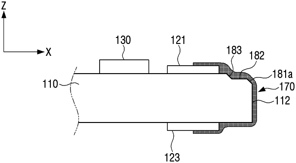
1. A display panel comprising: a thin film transistor substrate; a plurality of micro light emitting diodes (LEDs) arranged on one surface of the thin film transistor substrate; a plurality of first connection pads disposed on the one surface of the thin film transistor substrate; a plurality of second connection pads disposed on the other surface of the thin film transistor substrate that faces the one surface; and a plurality of connection wirings disposed on a side surface of the thin film transistor substrate for electrically connecting each of the plurality of first connection pads and the plurality of second connection pads, wherein at least one edge area of an edge area on the one surface and an edge area on the other surface of the thin film transistor substrate includes a cutting area which is cut in an inward direction of the thin film transistor substrate, wherein the cutting area is formed to have a multi-stage structure, the multi-stage structure comprising a plurality of cutting surfaces consecutively arranged between the side surface and the one surface or the other surface, wherein one or more of the cutting surfaces of the cutting area are formed by cutting or etching a portion of the cutting area between the side surface and the one surface or the other surface to receive a respective one of the plurality of connection wirings, and wherein the plurality of connection wirings are metal deposited along the multi-stage structure of the cutting area.
|
