| CPC H01L 33/0095 (2013.01) [H01L 21/6838 (2013.01); H01L 22/14 (2013.01); H01L 33/06 (2013.01); H01L 33/62 (2013.01); H01L 2933/0033 (2013.01); H01L 2933/0066 (2013.01)] | 20 Claims |
|
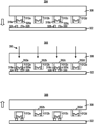
1. A method, comprising:
forming an epitaxial layer on a starter substrate;
attaching the epitaxial layer onto a carrier substrate;
etching away the starter substrate;
etching away part of the epitaxial layer to form a plurality of light emitting diode (LED) dies;
forming device-side bumps on the plurality of LED dies;
forming backplane-side bumps on at least one of one or more pre-determined locations on a backplane, the at least one of one or more pre-determined locations corresponding to one or more selected LED dies of the plurality of LED dies;
establishing one or more conductive bonds between the device-side bumps of the one or more selected LED dies and the corresponding backplane-side bumps on backplane; and
moving the carrier substrate away from the backplane to transfer the one or more LED dies to the backplane.
|