| CPC H01L 33/0095 (2013.01) [H01L 25/0753 (2013.01); H01L 33/0093 (2020.05); H01L 2933/0016 (2013.01)] | 20 Claims |

|
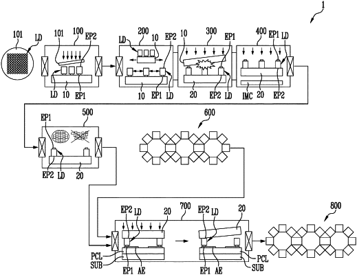
1. A manufacturing apparatus of a display device, comprising:
a first unit configured to transfer a plurality of light emitting elements on a growth substrate to a first film to be spaced from one another by a first distance;
a second unit configured to expand the first film to space each of the plurality of light emitting elements on the first film from adjacent light emitting elements by a second distance greater than the first distance;
a third unit configured to retransfer the plurality of light emitting elements to a second film;
a fourth unit configured to determine positions of the plurality of light emitting elements by irradiating a guide laser beam to the plurality of light emitting elements on the second film;
a fifth unit configured to bin the light emitting elements on the second film, and determine an effective light source from among the light emitting elements;
a sixth unit configured to form a plurality of pixels on a substrate, each pixel comprising one or more transistors, a first electrode electrically connected to a transistor from among the one or more transistors, and a first bonding electrode on the first electrode;
a seventh unit configured to remove the second film after transferring one light emitting element to the first bonding electrode of one pixel by irradiating a laser beam using a laser shot; and
an eighth unit configured to form a second electrode on the one light emitting element.
|