| CPC H01L 31/16 (2013.01) [H01L 31/024 (2013.01); H01L 33/62 (2013.01); H01L 33/644 (2013.01); H04B 10/40 (2013.01)] | 14 Claims |

|
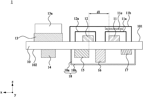
1. A semiconductor device package, comprising:
a substrate having a first surface and a second surface opposite to the first surface;
an optical device disposed on the first surface of the substrate; and
an electronic device disposed on the second surface of the substrate, wherein a power of the electronic device is greater than a power of the optical device;
a case disposed on the second surface of the substrate and defining a space for accommodating the electronic device; and
a first thermal paste connecting the case and the electronic device;
wherein a vertical projection of the optical device on the first surface is spaced apart from a vertical projection of the electronic device on the second surface by a distance greater than zero;
wherein the vertical projection of the optical device on the first surface overlaps with a vertical projection of the case on the second surface of the substrate.
|