| CPC H01L 29/7883 (2013.01) [H01L 21/26513 (2013.01); H01L 29/40114 (2019.08); H01L 29/41725 (2013.01); H01L 29/42324 (2013.01); H01L 29/66492 (2013.01); H01L 29/66825 (2013.01); H01L 29/7833 (2013.01); H10B 41/30 (2023.02)] | 20 Claims |

|
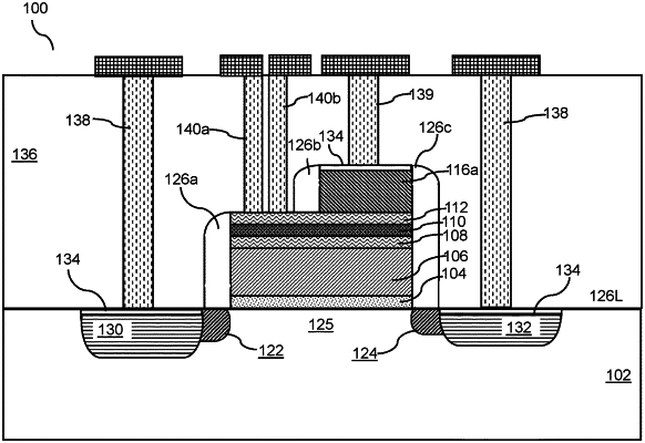
1. A method of making a flash memory device, comprising:
depositing a continuous tunnel dielectric layer over a substrate;
depositing a continuous floating gate layer over the continuous tunnel dielectric layer;
depositing a continuous control gate dielectric layer over the continuous floating gate layer;
depositing a continuous control gate layer over the continuous control gate dielectric layer;
patterning the continuous tunnel dielectric layer, the continuous floating gate layer, the continuous control gate dielectric layer and the continuous control gate layer by performing a first anisotropic etch process to form a patterned tunnel dielectric layer, a floating gate electrode, a patterned control gate dielectric layer and a control gate electrode;
further patterning the control gate electrode by performing a second anisotropic etch process to expose a surface of the patterned control gate dielectric layer and form a smaller length control gate electrode such that the smaller length control gate electrode has a length along a major axis of the smaller length control gate electrode that is less than a length of the floating gate electrode along a major axis of the floating gate electrode;
forming a source region and a drain region in the substrate; and
forming an electrical contact on the exposed surface of the patterned control gate dielectric layer, wherein the exposed surface of the control gate dielectric layer is over a channel region located between the source region and the drain region.
|