| CPC H01L 29/78642 (2013.01) [G11C 11/2257 (2013.01); G11C 11/4085 (2013.01); H01L 27/124 (2013.01); H01L 27/127 (2013.01); H01L 27/1222 (2013.01); H01L 27/1255 (2013.01); H01L 29/40111 (2019.08); H01L 29/42392 (2013.01); H01L 29/4908 (2013.01); H01L 29/516 (2013.01); H01L 29/6684 (2013.01); H01L 29/66742 (2013.01); H01L 29/78391 (2014.09); H01L 29/78618 (2013.01); H01L 29/78651 (2013.01); H10B 12/0335 (2023.02); H10B 12/315 (2023.02); H10B 12/50 (2023.02); H10B 51/30 (2023.02); H10B 51/40 (2023.02); H10B 53/30 (2023.02); H10B 53/40 (2023.02)] | 20 Claims |
|
1. A method of forming an integrated assembly, comprising:
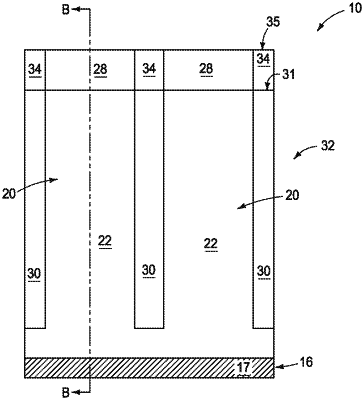
forming an arrangement to comprise semiconductor pillars extending upwardly from digit lines; the digits lines extending along a first direction;
patterning slits to extend partially into the pillars; each of the pillars having an associated one of the slits patterned therein and being configured to have a base region, and to have a pair of segments extending upwardly from the base region, with the segments of said pair being spaced from one another by an intervening gap corresponding to said associated one of the slits;
forming first insulative material along sidewalls of the slits;
forming conductive wordlines within the slits, adjacent the first insulative material, and extending along a second direction which crosses the first direction;
forming first source/drain regions within the base regions of the pillars;
forming second source/drain regions within the segments of the pillars, and vertically spaced from the first source/drain regions by channel regions;
forming second insulative material within the slits and over the wordlines; and
forming conductive interconnects within the slits and over the second insulative material.
|