| CPC H01L 29/7813 (2013.01) [H01L 29/1095 (2013.01); H01L 29/42368 (2013.01); H01L 29/66712 (2013.01)] | 20 Claims |

|
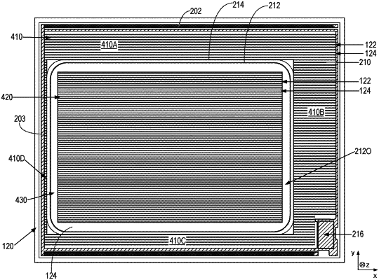
1. A MOSFET device die, comprising:
an active area including a first active area portion and a second active area portion formed on a semiconductor substrate; and
at least one mesa formed in the semiconductor substrate extending in a longitudinal direction through the active area, the at least one mesa including a channel region extending in a longitudinal direction, the channel region including low threshold voltage channel portions and high threshold voltage channel portions,
the first active area portion including the channel portions in a first ratio of low threshold voltage channel portions to high threshold voltage channel portions, and
the second active area portion including channel portions in a second ratio of low threshold voltage channel portions to high threshold voltage channel portions,
wherein the first ratio is larger than the second ratio.
|