| CPC H01L 29/7787 (2013.01) [H01L 29/0646 (2013.01); H01L 29/0649 (2013.01); H01L 29/2003 (2013.01); H01L 29/207 (2013.01); H01L 29/401 (2013.01); H01L 29/41766 (2013.01); H01L 29/66462 (2013.01); H01L 29/7786 (2013.01); H01L 29/205 (2013.01); H01L 29/452 (2013.01)] | 20 Claims |

|
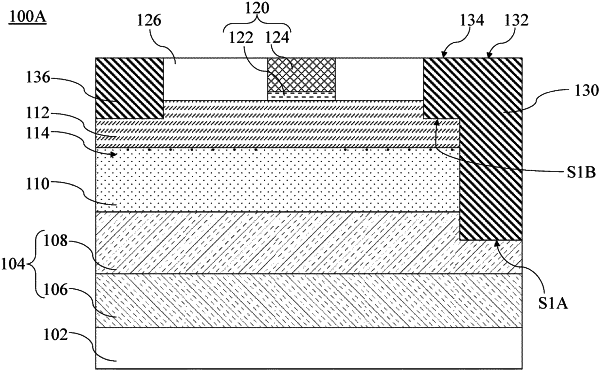
1. A nitride-based semiconductor device, comprising:
a substrate;
a buffer disposed over the substrate;
a first nitride-based semiconductor layer disposed over the buffer;
a shield layer disposed between the buffer and the first nitride-based semiconductor layer and comprising a first isolation compound that has a bandgap greater than a bandgap of the first nitride-based semiconductor layer, wherein the first isolation compound is made of at least one two-dimensional material which comprises at least one metal element;
a second nitride-based semiconductor layer disposed on the first nitride-based semiconductor layer and having a bandgap less than the bandgap of the first isolation compound and greater than the bandgap of the first nitride-based semiconductor layer; and
a pair of source/drain (S/D) electrodes and a gate electrode disposed over the second nitride-based semiconductor layer, wherein the gate electrode is present between the S/D electrodes, and vertical projections of the S/D electrodes and the gate electrode on the buffer are entirely within a vertical projection of the shield layer on the buffer.
|