| CPC H01L 29/7786 (2013.01) [H01L 21/28581 (2013.01); H01L 29/205 (2013.01); H01L 29/42316 (2013.01); H01L 29/66462 (2013.01)] | 14 Claims |
|
1. A method for manufacturing a field-effect transistor, comprising:
a first step of forming a buffer layer, a channel layer, a barrier layer, a carrier supply layer, and an ohmic cap layer on a semiconductor substrate;
a second step of forming a source electrode and a drain electrode on the ohmic cap layer; a third step of forming an insulating layer on the ohmic cap layer between the source electrode and the drain electrode;
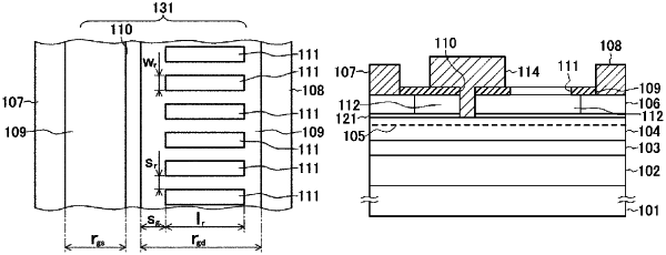
a fourth step of forming, in the insulating layer, a gate opening portion, wherein the gate opening portion is spaced at a greater distance from the drain electrode than from the source electrode, wherein the drain electrode is spaced apart from the source electrode along a gate length direction;
a fifth step of forming a plurality of asymmetric recess-forming opening portions, which are arranged in a row in a gate width direction between the gate opening portion and the drain electrode within the insulating layer, a respective opening size of each of the plurality of asymmetric recess-forming opening portions in the gate length direction being greater than a respective opening size of each of the plurality of asymmetric recess-forming opening portions in the gate width direction, the gate width direction being perpendicular to the gate length direction;
a sixth step of etching the ohmic cap layer using, as a mask, the insulating layer in which the gate opening portion and the plurality of asymmetric recess-forming opening portions are formed, and forming a recess region below the gate opening portion and the plurality of asymmetric recess-forming opening portions; and
a seventh step of forming a gate electrode on the insulating layer and disposed in the recess region and in the gate opening portion, wherein the gate electrode is joined to the barrier layer through a Schottky junction, and wherein, in the sixth step, an amount of etching of the ohmic cap layer on a drain electrode side relative to the gate opening portion is controlled based on the respective opening size of each of the plurality of asymmetric recess-forming opening portions in the gate length direction.
|
|
6. A field-effect transistor comprising:
a buffer layer, a channel layer, a barrier layer, a carrier supply layer, and an ohmic cap layer on a semiconductor substrate;
a first source electrode and a first drain electrode formed on the ohmic cap layer, wherein the first drain electrode is spaced apart from the first source electrode along a gate length direction;
an insulating layer on the ohmic cap layer between the first source electrode and the first drain electrode;
a first gate opening in the insulating layer between the first drain electrode and the first source electrode, wherein a distance of the first gate opening from the first drain electrode is greater than a distance of the first gate opening from the first source electrode;
a plurality of first asymmetric openings in the insulating layer between the first gate opening and the first drain electrode;
a first recess region below the first gate opening and the plurality of first asymmetric openings; and
a first gate electrode on the insulating layer and disposed in the first gate opening and the first recess region, wherein the first gate electrode is joined to the barrier layer through a first Schottky junction, wherein each of the plurality of first asymmetric openings is arranged such that an opening size thereof in the gate length direction is greater than an opening size thereof in a gate width direction, the gate width direction being perpendicular to the gate length direction.
|