| CPC H01L 29/7786 (2013.01) [H01L 29/1066 (2013.01); H01L 29/2003 (2013.01); H01L 29/205 (2013.01); H01L 29/41766 (2013.01); H01L 29/4236 (2013.01); H01L 29/66462 (2013.01)] | 5 Claims |

|
1. A manufacturing method of a semiconductor device, comprising:
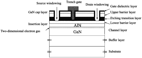
manufacturing and forming a semiconductor material layer comprising a heterojunction, wherein a two-dimensional electron gas is formed in the heterojunction, and the heterojunction comprises a first semiconductor layer and a second semiconductor layer, wherein the manufacturing and forming comprises growing a third semiconductor layer and a fourth semiconductor layer on the first semiconductor layer in sequence so as to form the second semiconductor layer, and setting an etching transition layer between the third semiconductor layer and the fourth semiconductor layer; and
etching parts of the semiconductor material layer, including a part of the fourth semiconductor layer, located in regions corresponding to a source, a drain and a gate, until the etching is stopped after reaching or entering the etching transition layer, then completely removing parts of the etching transition layer located in the regions corresponding to the source, the drain and the gate through thermal treatment, thereby forming trench structures respectively matched with the source, the drain and the gate;
after the trench structure matched with the gate is formed in the second semiconductor layer, cladding a dielectric layer on the semiconductor material layer on an inner wall of the trench structure matched with the gate, wherein the dielectric layer at least continuously covers trench walls of the trench structures matched with the source, the drain and the gate;
providing windows for allowing the source and the drain to pass on the dielectric layer; and
manufacturing the source, the drain and the gate, wherein the source, the drain, and the gate are matched with the semiconductor material layer, and wherein the gate is manufactured so that the dielectric layer is spaced between the gate and the third semiconductor.
|