| CPC H01L 29/66734 (2013.01) [H01L 21/26506 (2013.01); H01L 21/823412 (2013.01); H01L 21/823437 (2013.01); H01L 21/823475 (2013.01); H01L 21/823487 (2013.01); H01L 27/088 (2013.01); H01L 29/0878 (2013.01); H01L 29/1033 (2013.01); H01L 29/1095 (2013.01); H01L 29/36 (2013.01); H01L 29/407 (2013.01); H01L 29/41741 (2013.01); H01L 29/41766 (2013.01); H01L 29/4236 (2013.01); H01L 29/66727 (2013.01); H01L 29/7395 (2013.01); H01L 29/7803 (2013.01); H01L 29/7813 (2013.01); H01L 29/7827 (2013.01); H01L 29/7831 (2013.01); H01L 29/7835 (2013.01); H01L 29/0847 (2013.01); H01L 29/42368 (2013.01); H01L 29/66666 (2013.01)] | 19 Claims |

|
5. A power semiconductor device, comprising:
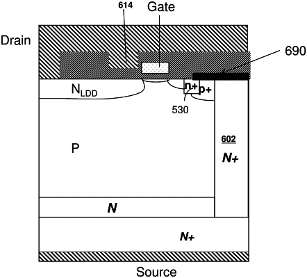
a first and a second laterally-gated transistor both having a portion of a first-conductivity-type source region, a gate electrode which is capacitively coupled to a body region to selectably form a lateral channel therein, a first-conductivity-type drain extension region connecting said lateral channel to a common drain electrode, a vertically-extended source extension region connecting said source region to a common source electrode on the backside of the device, and a shorting strap connecting said source region to said vertically-extended source extension region;
wherein both said gate electrodes are electrically separate portions of a single thin film layer;
wherein the threshold voltage of said first laterally-gated transistor is less than the threshold voltage of said second laterally-gated transistor; and
wherein said first laterally-gated transistor has a width which is smaller than a width of said second laterally-gated transistor.
|