US 11,888,045 B2
Integrated dipole flow for transistor
Yongjing Lin, San Jose, CA (US); Karla M Bernal Ramos, San Jose, CA (US); Luping Li, Santa Clara, CA (US); Shih Chung Chen, Cupertino, CA (US); Jacqueline S. Wrench, San Jose, CA (US); Yixiong Yang, Fremont, CA (US); Steven C. H. Hung, Sunnyvale, CA (US); Srinivas Gandikota, Santa Clara, CA (US); Naomi Yoshida, Sunnyvale, CA (US); and Lin Dong, San Jose, CA (US)
Assigned to Applied Materials, Inc., Santa Clara, CA (US)
Filed by Applied Materials, Inc., Santa Clara, CA (US)
Filed on Dec. 21, 2021, as Appl. No. 17/557,787.
Application 17/557,787 is a continuation of application No. 16/876,276, filed on May 18, 2020, granted, now 11,245,022.
Claims priority of provisional application 62/852,349, filed on May 24, 2019.
Prior Publication US 2022/0115516 A1, Apr. 14, 2022
Int. Cl. H01L 29/51 (2006.01); H01L 29/40 (2006.01); H01L 29/49 (2006.01)
CPC H01L 29/513 (2013.01) [H01L 29/401 (2013.01); H01L 29/4958 (2013.01); H01L 29/4966 (2013.01)] 16 Claims
OG exemplary drawing
 
1. An electronic device comprising:
a source region, a drain region and a channel separating the source region and drain region; and
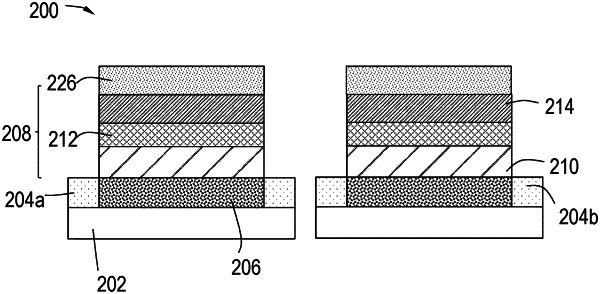
a dipole region on a top surface of the channel, the dipole region comprising an interlayer dielectric, a high-κ dielectric material, and a dipole layer, the dipole layer deposited by atomic layer deposition (ALD) at a temperature in a range of from 200° C. to about 500° C. of alternating cycles of titanium nitride (TiN) and a dipole precursor, the dipole layer comprising one or more of titanium lanthanum nitride (TiLaN), titanium yttrium nitride (TiYN), titanium strontium nitride (TiSrN), or titanium magnesium nitride (TiMgN).