| CPC H01L 29/407 (2013.01) [H01L 29/0649 (2013.01); H01L 29/0661 (2013.01); H01L 29/1608 (2013.01); H01L 29/2003 (2013.01); H01L 29/6606 (2013.01); H01L 29/66143 (2013.01); H01L 29/8613 (2013.01); H01L 29/872 (2013.01)] | 15 Claims |
|
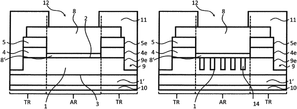
1. A power semiconductor device comprising:
a wide-bandgap semiconductor layer having a first main side and a second main side opposite to the first main side, wherein the first main side and the second main side extend in a lateral direction and wherein the wide-bandgap semiconductor layer comprises an active region and a termination region that laterally surrounds the active region, wherein the wide-bandgap semiconductor layer has a first recess that is recessed from the first main side in the termination region and surrounds the active region and wherein the wide-bandgap semiconductor layer also has a second recess that is recessed from the first main side in the active region and is filled with an insulating material, a depth of the second recess being the same as a depth of the first recess;
a field plate on the first main side of the wide-bandgap semiconductor layer over a first portion of the termination region, the field plate exposing the active region and a second portion of the wide-bandgap semiconductor layer in the termination region; and
a dielectric layer interposed between the field plate and the wide-bandgap semiconductor layer to separate the field plate from the wide-bandgap semiconductor layer;
wherein a sidewall of the first recess adjacent to the active region is laterally aligned with a circumferential edge of the field plate such that in an orthogonal projection onto a plane parallel to the first main side, an edge of the first recess defined by an upper end of the sidewall is within less than 1 nm from the circumferential edge of the field plate.
|