| CPC H01L 27/14649 (2013.01) [H01L 27/14689 (2013.01); H01L 27/14698 (2013.01); H01L 31/0312 (2013.01); H01L 31/107 (2013.01); H01L 31/1812 (2013.01); H01L 31/1864 (2013.01); H01L 31/1892 (2013.01)] | 13 Claims |
|
1. A short-wave infrared (SWIR) detector array defining an incident light surface and a lower surface opposite to said incident light surface, the SWIR detector array comprising:
at least one SWIR absorbing layer configured to convert, in electrical charges, electromagnetic waves having a wavelength comprised between 1.0 μm and 3.0 μm;
a p-n junction;
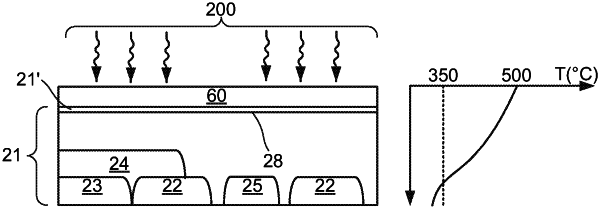
an annealed crystalline buffer layer; and
a doped readout wafer disposed in relation to the SWIR absorbing layer opposite to said incident light surface and separated from said SWIR absorbing layer by the annealed crystalline buffer layer, the doped readout wafer being either p-doped or n-doped, the doped readout wafer having a deposition surface, the doped readout wafer comprising
at least one charge collecting area that is one of p-doped and n-doped, and
a complementary metal-oxide semiconductor (CMOS) electrical circuit,
said annealed crystalline buffer layer being disposed on the deposition surface and being at least partially made of germanium (Ge), the annealed crystalline buffer layer comprising an oxide-free surface to a side away from said doped readout wafer, the annealed crystalline buffer layer having a crystalline structure that overcomes differences of lattice and dilatation coefficients between said doped readout wafer and said at least one SWIR absorbing layer,
said at least one SWIR absorbing layer being disposed on said oxide-free surface, said at least one SWIR absorbing layer being at least partially made of germanium (Ge) and tin (Sn).
|