| CPC H01L 27/14643 (2013.01) [H01L 27/14623 (2013.01); H04N 25/76 (2023.01)] | 20 Claims |
|
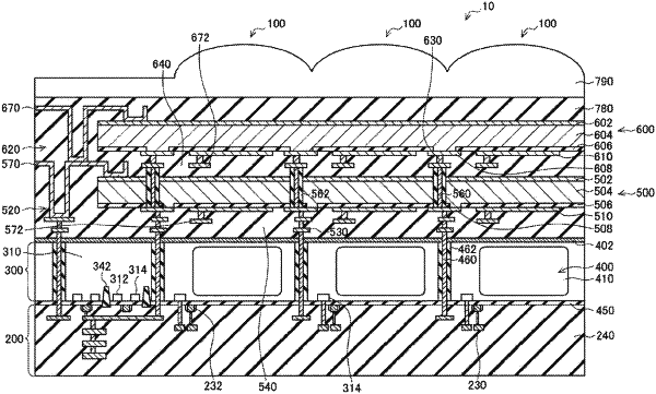
1. A solid-state image capturing element comprising:
a semiconductor substrate;
a first photoelectric conversion part provided above the semiconductor substrate and configured to convert light into electric charge; and
a second photoelectric conversion part provided above the first photoelectric conversion part and configured to convert light into electric charge, wherein
the first and the second photoelectric conversion parts each have a laminated structure including
an upper electrode,
a lower electrode,
a photoelectric conversion film sandwiched between the upper electrode and the lower electrode, and
an accumulation electrode facing the upper electrode through the photoelectric conversion film and an insulating film, and
the lower electrode of each of the first and the second photoelectric conversion parts is electrically connected with a common electric charge accumulation part through a common penetration electrode provided in common to the first and the second photoelectric conversion parts and penetrating through the semiconductor substrate, the common electric charge accumulation part being provided in common to the first and the second photoelectric conversion parts in the semiconductor substrate.
|