| CPC H01L 27/14623 (2013.01) [H01L 27/1463 (2013.01); H01L 27/1464 (2013.01); H01L 27/14614 (2013.01); H01L 27/14627 (2013.01); H01L 27/14643 (2013.01); H01L 27/14683 (2013.01)] | 12 Claims |
|
1. An imaging device, comprising:
a substrate;
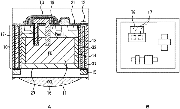
a plurality of photoelectric conversion elements in the substrate, wherein each of the plurality of photoelectric conversion elements includes an N-type region that performs photoelectric conversion;
a light-shielding wall between a first photoelectric conversion element and a second photoelectric conversion element of the plurality of photoelectric conversion elements in the substrate in a cross-sectional view;
a first P-type region between the first photoelectric conversion element and the light-shielding wall in the cross-sectional view;
a second P-type region adjacent to the first P-type region and between the first photoelectric conversion element and a light incident side of the substrate in the cross-sectional view; and
a vertical-type transistor extending in a depth direction of the substrate in the cross-sectional view, wherein a gate of the vertical-type transistor includes two trench-type electrodes.
|