| CPC H01L 27/14623 (2013.01) [H01L 27/1469 (2013.01); H01L 27/14612 (2013.01); H01L 27/14634 (2013.01); H01L 27/14636 (2013.01); H01L 27/14643 (2013.01); H01L 27/14689 (2013.01)] | 15 Claims |

|
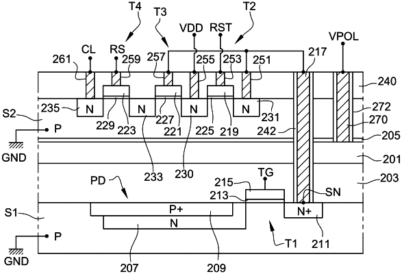
1. An image sensor comprising a plurality of pixels, each pixel comprising a photodetector and a control circuit for controlling the photodetector, the photodetector being formed inside and on top of a first semiconductor substrate, and the control circuit comprising at least one first MOS transistor formed inside and on top of a second semiconductor substrate arranged on the first semiconductor substrate, the image sensor being intended to be illuminated on the side of the surface of the first semiconductor substrate opposite to the second semiconductor substrate, the image sensor further comprising a shield arranged between the first and second semiconductor substrates and extending over substantially the entire surface of the image sensor, said shield comprising at least one electrically-conductive layer,
wherein the control circuit comprises at least one second MOS transistor formed inside and on top of the first semiconductor substrate, and wherein the gate of said at least one second MOS transistor is arranged on the side of a surface of the first semiconductor substrate facing the second semiconductor substrate, the gate of said at least one first MOS transistor being arranged on the side of a surface of the second semiconductor substrate opposite to the first semiconductor substrate,
wherein said at least one conductive layer of the shield is connected to a node of application of a bias potential via a conductive via crossing the second semiconductor substrate.
|