| CPC H01L 27/14623 (2013.01) [H01L 27/1463 (2013.01); H01L 27/14643 (2013.01); H01L 27/14685 (2013.01)] | 17 Claims |
|
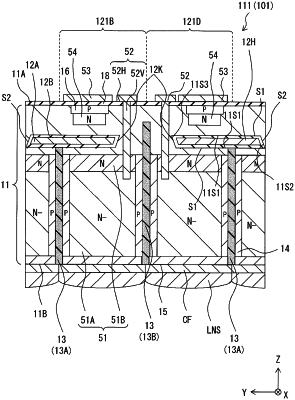
1. An imaging device comprising:
a Si {111} substrate having a first direction as a thickness direction and including a first crystal plane represented by a plane index {111} extending along a horizontal plane orthogonal to the first direction;
a photoelectric conversion section provided in the Si {111} substrate;
a first conductivity type region provided in the Si {111} substrate; and
a light-shielding section including a horizontal light-shielding part and a vertical light-shielding part, the horizontal light-shielding part positioned between the photoelectric conversion section and the first conductivity type region in the first direction and extending along the horizontal plane, the vertical light-shielding part being orthogonal to the horizontal light-shielding part;
the horizontal light-shielding part comprising an insulating material including:
a first plane formed along the first crystal plane of the Si {111} substrate orthogonal to the first direction, and
a second plane formed along a second crystal plane of the Si {111} substrate being inclined relative to the first direction and represented by the plane index {111}.
|