| CPC H01L 27/1218 (2013.01) [H01L 27/127 (2013.01); H01L 27/1225 (2013.01); H10K 59/122 (2023.02); H10K 59/123 (2023.02)] | 18 Claims |
|
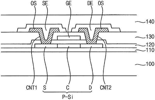
1. A display apparatus, comprising:
a base substrate;
a first active pattern disposed on the base substrate, the first active pattern including polycrystalline silicon;
a gate electrode overlapping a first portion of the first active pattern;
at least one first insulation layer disposed on the gate electrode;
a source electrode electrically connected to a second portion of the first active pattern and a drain electrode electrically connected to a third portion of the first active pattern;
a second active pattern disposed on the first insulation layer, the second active pattern including an oxide semiconductor; and
an oxide semiconductor pattern disposed between the source electrode and the second portion of the first active pattern and between the drain electrode and the third portion of the first active pattern, the oxide semiconductor pattern directly contacting the second and third portions of the first active pattern, wherein
the first portion of the first active pattern is a channel of a transistor, the second portion of the first active pattern is a source of the transistor, the third portion of the first active pattern is a drain of the transistor.
|