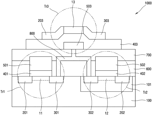
| CPC H01L 27/1207 (2013.01) [G06N 3/063 (2013.01); G06N 3/08 (2013.01)] | 24 Claims |

|
1. A semiconductor device comprising:
a first transistor including a first channel layer of a first conductivity type;
a second transistor provided in parallel with the first transistor, the second transistor including a second channel layer of a second conductivity type; and
a third transistor stacked on the first transistor and the second transistor, the third transistor including a third channel layer and a gate electrode that are spaced apart from each other in a thickness direction with a gate insulating film therebetween, the gate insulating film including a ferroelectric material, wherein
the third channel layer is laterally between a source electrode of the third transistor and a drain electrode of the third transistor such that third channel layer contacts a sidewall of the source electrode of the third transistor and a sidewall of the drain electrode of the third transistor,
the gate electrode is spaced apart vertically from the third channel layer, does not vertically overlap the source electrode of the third transistor, and does not vertically overlap the drain electrode of the third transistor,
the ferroelectric material includes at least one of HfO, HfxZr1-xO, and ZrO, and
the ferroelectric material is doped with at least one of Si, Al, Zr, Y, La, Gd, Sr, and Hf.
|
|
14. A neuromorphic circuit comprising:
pre-synaptic neuron circuits;
pre-synaptic lines extending in a first direction from the pre-synaptic neuron circuits;
post synaptic neuron circuits;
post synaptic lines extending from the post synaptic neuron circuits in a second direction crossing the first direction; and
synaptic circuits provided at intersections of the pre-synaptic lines and the post synaptic lines,
the synaptic circuits each including a first transistor, a second transistor, and a third transistor on a substrate,
the first transistor including a first channel layer of a first conductivity type,
the second transistor having a second channel layer of a second conductivity type,
the first transistor and the second transistor being parallel with each other on the substrate,
the third transistor being stacked on the first transistor and the second transistor,
the third transistor including a third channel layer and a gate electrode that are spaced apart from each other in a thickness direction with a gate insulating film therebetween,
the gate insulating film including a ferroelectric material,
the third channel layer is laterally between a source electrode of the third transistor and a drain electrode of the third transistor such that third channel layer contacts a sidewall of the source electrode of the third transistor and a sidewall of the drain electrode of the third transistor,
the gate electrode is spaced apart vertically from the third channel layer, does not vertically overlap the source electrode of the third transistor, and does not vertically overlap the drain electrode of the third transistor,
the ferroelectric material including at least one of HfO, HfxZr1-xO, and ZrO, and
the ferroelectric material being doped with at least one of Si, Al, Zr, Y, La, Gd, Sr, and Hf.
|
|
20. A semiconductor device comprising:
a CMOS circuit including a first transistor of a first conductivity type and a second transistor of a second conductivity type;
a third transistor including a gate electrode, a channel, and a gate insulating film, the gate insulating film including a ferroelectric material; and
a contact electrode connected to the gate electrode of the third transistor, a drain of the first transistor, and a drain of the second transistor, wherein
the channel of the third transistor is laterally between a source electrode of the third transistor and a drain electrode of the third transistor such that the channel of the third transistor contacts a sidewall of the source electrode of the third transistor and a sidewall of the drain electrode of the third transistor,
the gate electrode is spaced apart vertically from the channel, does not vertically overlap the source electrode of the third transistor, and does not vertically overlap the drain electrode of the third transistor,
the ferroelectric material includes at least one of HfO, HfxZr1-xO, and ZrO, and
the ferroelectric material is doped with at least one of Si, Al, Zr, Y, La, Gd, Sr, and Hf.
|