| CPC H01L 27/1207 (2013.01) [H01L 29/0847 (2013.01); H01L 29/1033 (2013.01); H01L 29/41733 (2013.01); H01L 29/66742 (2013.01)] | 17 Claims |
|
1. An integrated circuit (IC) structure, comprising:
one or more levels of metallization; and
a transistor structure over at least one of the levels of metallization, the transistor structure comprising:
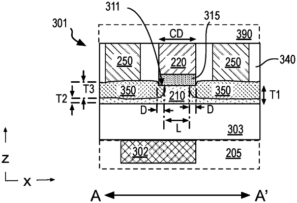
a source material separated from a drain material by a first length of channel material, wherein the channel material has a first composition comprising a Group IV, a Group III-V, or metal oxide material, and the source material and the drain material have a second composition, different than the first composition, and comprising Sn as a majority constituent and one or more p-type impurities;
a gate electrode separated from the channel, source, and drain materials by one or more gate dielectric materials, wherein the gate electrode has a second length, in a direction parallel to the first length, that is larger than the first length; and
a source contact metallization coupled to the source material, and a drain contact metallization coupled to the drain material.
|