| CPC H01L 27/0924 (2013.01) [H01L 21/26506 (2013.01); H01L 21/823807 (2013.01); H01L 21/823821 (2013.01); H01L 21/84 (2013.01); H01L 27/092 (2013.01); H01L 27/1203 (2013.01); H01L 29/0649 (2013.01); H01L 29/1054 (2013.01); H01L 29/16 (2013.01); H01L 29/1606 (2013.01); H01L 29/24 (2013.01); H01L 29/267 (2013.01); H01L 29/41791 (2013.01); H01L 29/4232 (2013.01); H01L 29/66045 (2013.01); H01L 29/66795 (2013.01); H01L 29/7391 (2013.01); H01L 29/778 (2013.01); H01L 29/7851 (2013.01); H01L 29/78618 (2013.01); H01L 29/78639 (2013.01); H01L 29/78681 (2013.01); H01L 29/78684 (2013.01); H01L 29/78696 (2013.01); H10B 10/00 (2023.02)] | 20 Claims |
|
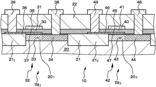
1. A complementary transistor, comprising:
a semiconductor substrate;
a first transistor including:
a first control electrode;
a first active region located below the first control electrode;
a first A extension region extending from one end of the first active region;
a first B extension region extending from the other end of the first active region; and
a buffer layer provided between the first control electrode and the semiconductor substrate; and
a second transistor including:
a second control electrode;
a second active region located below the second control electrode;
a second A extension region extending from one end of the second active region; and
a second B extension region extending from the other end of the second active region.
|