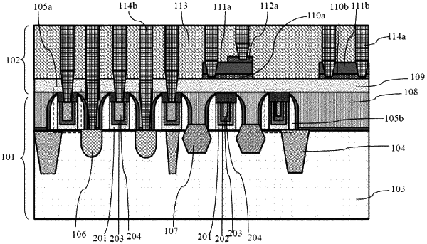
| CPC H01L 27/0629 (2013.01) [H01L 23/5223 (2013.01); H01L 23/5228 (2013.01); H01L 28/20 (2013.01); H01L 28/60 (2013.01); H01L 29/66795 (2013.01); H01L 29/7851 (2013.01)] | 9 Claims |

|
1. A method for fabricating a capacitor integrated in a FinFET device, wherein the method comprises following steps:
step 1: providing a semiconductor substrate which has completed a front-end-of-line process, wherein a layer formed in the front-end-of-line process comprises the FinFET device, wherein the FinFET device comprises gate structures, source regions and drain regions placed on two sides of the gate structures, wherein the layer formed in the front-end-of-line process further comprises a zeroth interlayer film filled between the gate structures, wherein top surfaces of the gate structures are in flush with a surface of the zeroth interlayer film; and
step 2: performing a middle-end-of-line process and forming a capacitor and a resistor in the middle-end-of-line process layer;
wherein the middle-end-of-line process comprises following sub-steps:
step 2-1: forming a first oxide layer on top surfaces of the gate structures and the zeroth interlayer film;
step 2-2: forming a first TiN layer and a second dielectric layer sequentially on the surface of the first oxide layer;
step 2-3: performing photolithography with a first photomask to form a first photoresist mask, wherein the first photoresist mask covers forming regions of the capacitor and the resistor and keeps remaining regions besides the forming regions of the capacitor and the resistor open;
step 2-4: etching the second dielectric layer and the first TiN layer sequentially; wherein after the etching, the first TiN layer becomes a lower electrode plate and the second dielectric layer forms an intermediate dielectric layer of the capacitor in the forming region of the capacitor, and the first TiN layer forms a resistor main body layer and the second dielectric layer forms a resistor cover layer in the forming region of the resistor;
step 2-5: forming a second TiN layer;
step 2-6: performing photolithography with a second photomask to form a second photoresist mask, wherein the second photoresist mask covers a forming region of the upper electrode plate of the capacitor and keeps remaining regions besides a forming region of the upper electrode plate open;
step 2-7: etching the second TiN layer to form the upper electrode plate, wherein an area of the upper electrode plate is configured to be smaller than an area of the lower electrode plate;
step 2-8: forming a first interlayer film, wherein the first interlayer film is disposed on the surface of the first oxide layer which is under the capacitor and the resistor; and
step 2-9: patterning a metal zeroth layer in the first interlayer film, wherein the lower electrode plate, the upper electrode plate and the resistor main body layer are respectively connected with a metal zeroth main layer of the metal zeroth layer.
|