| CPC H01L 27/0255 (2013.01) [G09G 3/20 (2013.01); H01L 23/482 (2013.01); H01L 23/485 (2013.01); H01L 29/42376 (2013.01); H01L 29/45 (2013.01); H01L 29/66969 (2013.01); H01L 29/7391 (2013.01); H01L 29/861 (2013.01); H01L 29/872 (2013.01); G09G 2300/0885 (2013.01); G09G 2330/04 (2013.01); G09G 2330/08 (2013.01); H01L 29/0688 (2013.01); H01L 29/0692 (2013.01); H01L 29/24 (2013.01)] | 4 Claims |

|
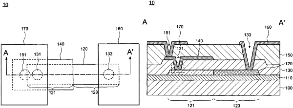
1. A diode comprising:
a semiconductor layer including a first region and a second region;
a first insulating layer covering the semiconductor layer;
a first conductive layer arranged above the first insulating layer; and
a second conductive layer arranged above the first insulating layer,
wherein
a first aperture is formed in the insulating layer overlapped with the first region,
a second aperture is formed in the insulating layer overlapped with the second region,
a resistance of the semiconductor layer in the second region is different from a resistance of the semiconductor layer in the first region,
the first conductive layer connects to the semiconductor layer in the first aperture and overlapping with the semiconductor layer in the first region in a planar view,
the second conductive layer connects to the semiconductor layer in the second aperture,
a boundary between the first region and the second region is along a part of a pattern end of the first conductive layer in a planar view.
|