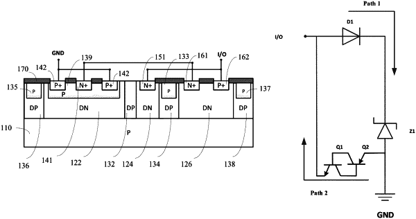
| CPC H01L 27/0255 (2013.01) [H01L 27/0262 (2013.01); H01L 27/0296 (2013.01); H01L 29/66106 (2013.01); H01L 29/866 (2013.01)] | 15 Claims |

|
1. A transient voltage suppression device, comprising:
a substrate, the substrate being of a second conductivity type;
a first conductivity type well region disposed in the substrate and comprising a first well,
a second well, and a third well;
a second conductivity type well region disposed in the substrate and comprising a fourth well and a fifth well, the fourth well being disposed between the first well and the second well to isolate the first well and the second well from each other, the fifth well being disposed between the second well and the third well to isolate the second well and the third well from each other, the first conductivity type and the second conductivity type being conductivity types opposite to each other;
a Zener diode well region being of the second conductivity type and disposed in the first well such that the Zener diode well region is isolated from the substrate through the first well;
a first doped region being of the first conductivity type and disposed in the Zener diode well region;
a second doped region being of the second conductivity type and disposed in the Zener diode well region;
a third doped region being of the first conductivity type and disposed in the second well;
a fourth doped region being of the first conductivity type and disposed in the third well; and
a fifth doped region being of the second conductivity type and disposed in the third well; wherein the third doped region, the second well, the fourth well, the first well, the Zener diode well region, and the second doped region constitute a silicon-controlled rectifier, the second doped region being used as an anode region of the silicon-controlled rectifier, the third doped region being used as a cathode region of the silicon-controlled rectifier, the second doped region being used as a first potential terminal, the first doped region being used as a cathode of a Zener diode, the Zener diode well region is used as an anode of the Zener diode, the fifth doped region is used as an anode of a first diode, the fourth doped region is used as a cathode of the first diode, the fifth doped region and the third doped region being electrically connected to each other and being used as a second potential terminal, the fourth doped region being electrically connected to the first doped region,
wherein the Zener diode and the first diode are connected in series, with the cathode region of the Zener diode connecting to the cathode of the first diode, the serially connected Zener diode and the first diode being connected with the silicon-controlled rectifier in parallel; and
wherein the first well, the fourth well, and the second well constitute a lateral NPN transistor of the silicon-controlled rectifier.
|