| CPC H01L 27/01 (2013.01) [H01L 25/0657 (2013.01); H01L 23/49816 (2013.01); H01L 23/585 (2013.01); H01L 28/40 (2013.01); H01L 2225/0652 (2013.01); H01L 2225/06517 (2013.01); H01L 2225/06572 (2013.01)] | 10 Claims |
|
1. A semiconductor package, comprising:
a package substrate;
a semiconductor die mounted on a top surface of the package substrate;
a plurality of conductive elements disposed on a bottom surface of the package substrate; and
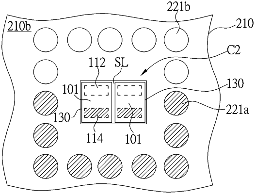
a land-side silicon capacitor disposed on the bottom surface of the package substrate and surrounded by the plurality of conductive elements, wherein the land-side silicon capacitor comprises at least two silicon capacitor unit dies adjoined to each other with an integral scribe line region, wherein the land-side silicon capacitor is surrounded by an annular, ring-shaped arrangement of conductive terminals comprising a first half-ring of ground conductive terminals arranged in proximity to anode terminals of the at least two silicon capacitor unit dies and a second half-ring of power conductive terminals arranged in proximity to cathode terminals of the at least two silicon capacitor unit dies.
|