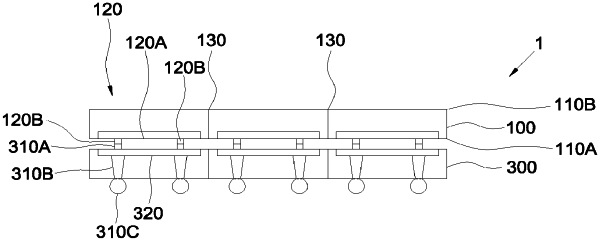
| CPC H01L 25/18 (2013.01) [H01L 24/13 (2013.01); H01L 24/16 (2013.01); H01L 24/94 (2013.01); H01L 25/50 (2013.01); H01L 2224/13025 (2013.01); H01L 2224/16146 (2013.01); H01L 2224/16148 (2013.01)] | 9 Claims |

|
1. A method of operating a microelectronic package, comprising a processing device stacking vertically with at least one memory device, the method comprising steps of:
reading data stored in a plurality of memory cells of a plurality of memory units of the memory device, with the processing device, with a plurality of signal channels each of which is dedicated to transmit signals from the processing device to one of the memory units and vice versa;
performing a test, with the processing device, on the memory cells in the memory units of the at least one memory device; and
indicating a failure found with the test, with the processing device.
|