| CPC H01L 25/0657 (2013.01) [H01L 24/16 (2013.01); H01L 24/32 (2013.01); H01L 24/48 (2013.01); H01L 24/73 (2013.01); H01L 24/81 (2013.01); H01L 24/85 (2013.01); H01L 25/50 (2013.01); H01L 23/3128 (2013.01); H01L 2224/05571 (2013.01); H01L 2224/05573 (2013.01); H01L 2224/05599 (2013.01); H01L 2224/1134 (2013.01); H01L 2224/13144 (2013.01); H01L 2224/13147 (2013.01); H01L 2224/16148 (2013.01); H01L 2224/32225 (2013.01); H01L 2224/4554 (2013.01); H01L 2224/45099 (2013.01); H01L 2224/4846 (2013.01); H01L 2224/48091 (2013.01); H01L 2224/48149 (2013.01); H01L 2224/48227 (2013.01); H01L 2224/48235 (2013.01); H01L 2224/48464 (2013.01); H01L 2224/48471 (2013.01); H01L 2224/48479 (2013.01); H01L 2224/48496 (2013.01); H01L 2224/73207 (2013.01); H01L 2224/73253 (2013.01); H01L 2224/73265 (2013.01); H01L 2224/85051 (2013.01); H01L 2224/85951 (2013.01); H01L 2224/85986 (2013.01); H01L 2225/0651 (2013.01); H01L 2225/0652 (2013.01); H01L 2225/06513 (2013.01); H01L 2225/06527 (2013.01); H01L 2225/06541 (2013.01); H01L 2225/06548 (2013.01); H01L 2924/00014 (2013.01); H01L 2924/01079 (2013.01); H01L 2924/15311 (2013.01); H01L 2924/181 (2013.01); Y10T 29/49144 (2015.01); Y10T 29/49149 (2015.01)] | 20 Claims |
|
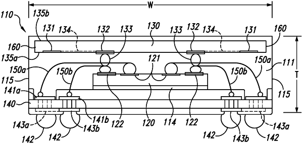
1. A microfeature device assembly, comprising:
a first die having a first bond pad surface, wherein the first bond pad surface includes a plurality of first device bond pads aligned along a first axis, a plurality of first intermediate bond pads aligned along a second axis, and a plurality of wirebond pads, wherein:
a first subset of the plurality of wirebond pads are electrically coupled to a corresponding pair from the plurality of first device bond pads and the plurality of first intermediate bond pads,
a second subset of the plurality of wirebond pads are each electrically coupled to an individual one of the plurality of first device bond pads, and
a third subset of the plurality of wirebond pads are each electrically coupled to an individual one of the plurality of first intermediate device bond pads;
a second die carried by the first die and having a second bond pad surface facing the first bond pad surface, wherein the second bond pad surface includes a plurality of second device bond pads each vertically aligned with a corresponding one of the plurality of first intermediate bond pads along the second axis and a plurality of second intermediate bond pads each vertically aligned with a corresponding one of the plurality of first device bond pads along the first axis; and
a conductive member disposed on each of the plurality of first intermediate bond pads and individually coupling the plurality of first intermediate bond pads to the plurality of second device bond pads.
|