| CPC H01L 25/0657 (2013.01) [H01L 23/481 (2013.01); H01L 24/05 (2013.01); H01L 24/08 (2013.01); H01L 24/16 (2013.01); H01L 24/48 (2013.01); H01L 25/18 (2013.01); H01L 2224/05147 (2013.01); H01L 2224/08145 (2013.01); H01L 2224/16227 (2013.01); H01L 2224/48227 (2013.01); H01L 2225/06541 (2013.01)] | 20 Claims |
|
1. A semiconductor package, comprising:
a first structure comprising a first semiconductor chip comprising a first semiconductor integrated circuit; and
a second structure on the first structure,
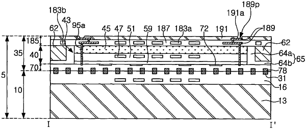
wherein the second structure comprises a second semiconductor chip comprising a second semiconductor integrated circuit, a semiconductor pattern horizontally spaced apart from the second semiconductor chip and on a side surface of the second semiconductor chip, an insulating gap fill pattern between the second semiconductor chip and the semiconductor pattern, and through-electrode structures,
wherein at least one of the through-electrode structures penetrates through at least a portion of the second semiconductor chip or penetrates through the semiconductor pattern, and wherein the semiconductor pattern is free of a semiconductor integrated circuit at a same height level as the second semiconductor integrated circuit of the second semiconductor chip.
|