| CPC H01L 24/24 (2013.01) [H01L 23/4951 (2013.01); H01L 23/49513 (2013.01); H01L 24/19 (2013.01); H01L 24/25 (2013.01); H01L 2224/2405 (2013.01); H01L 2224/24246 (2013.01); H01L 2224/2505 (2013.01); H01L 2224/25175 (2013.01); H01L 2924/182 (2013.01)] | 18 Claims |

|
1. A semiconductor device, comprising:
a support substrate;
electrically-conductive leads arranged around the support substrate, the electrically-conductive leads comprising respective proximal portions facing towards said support substrate and respective distal portions facing away from said support substrate;
a semiconductor die arranged onto said support substrate and onto the proximal portions of one or more of said electrically-conductive leads, the semiconductor die comprising a set of bonding pads at a front surface thereof which is opposed to the support substrate;
a layer of laser-activatable material molded onto said semiconductor die and said electrically-conductive leads; and
electrically-conductive formations, wherein said electrically-conductive formations comprise:
i) first electrically-conductive vias extending between said set of bonding pads at said front surface of the semiconductor die and a front surface of said layer of laser-activatable material;
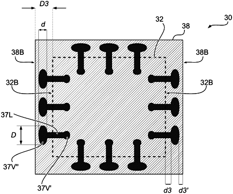
ii) second electrically-conductive vias extending between said distal portions of said electrically-conductive leads and the front surface of said layer of laser-activatable material, wherein said second electrically-conductive vias have an oval cross-section having a minor axis extending in a direction perpendicular to a respective side wall of the semiconductor die and a major axis extending in a direction parallel to said respective side wall of the semiconductor die and to said front surface of the semiconductor die; and
iii) electrically-conductive lines extending at said front surface of said layer of laser-activatable material and connecting selected first electrically-conductive vias to selected second electrically-conductive vias.
|