| CPC H01L 24/13 (2013.01) [H01L 24/05 (2013.01); H01L 2224/0401 (2013.01); H01L 2224/05001 (2013.01); H01L 2224/13099 (2013.01); H01L 2924/014 (2013.01); H01L 2924/3651 (2013.01)] | 20 Claims |
|
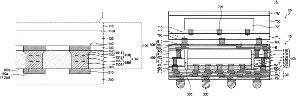
1. A method of manufacturing semiconductor device, the method comprising:
forming an under-bump pattern and a protective layer on a semiconductor substrate;
forming a seed layer on the under-bump pattern and the protective layer;
forming a resist pattern comprising a guide opening on the seed layer, the guide opening exposing at least a portion of a top surface of the seed layer which overlaps the under-bump pattern;
forming a preliminary bump pattern in the guide opening of the resist pattern; and
performing an annealing process to the preliminary bump pattern.
|