| CPC H01L 24/13 (2013.01) [H01L 24/05 (2013.01); H01L 24/16 (2013.01); H01L 24/81 (2013.01); H01L 2224/05644 (2013.01); H01L 2224/05647 (2013.01); H01L 2224/05655 (2013.01); H01L 2224/05664 (2013.01); H01L 2224/1308 (2013.01); H01L 2224/13144 (2013.01); H01L 2224/13147 (2013.01); H01L 2224/13155 (2013.01); H01L 2224/13164 (2013.01); H01L 2224/1601 (2013.01); H01L 2224/16145 (2013.01); H01L 2224/81815 (2013.01)] | 19 Claims |

|
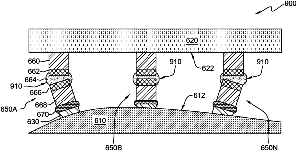
1. A method of interconnecting a first semiconductor structure with a second semiconductor structure, the method comprising:
forming a plurality of pillars on a surface of the first semiconductor structure, wherein each pillar in the plurality of pillars is formed by:
depositing a first metal layer onto a surface of the first semiconductor structure;
depositing a first solder layer onto the first metal layer;
depositing a second metal layer onto the first solder layer; and
depositing a second solder layer onto the second metal layer inverting the first semiconductor structure having the plurality of pillars formed on the surface of the first semiconductor; and
interconnecting the inverted first semiconductor structure with the second semiconductor structure by attaching the second solder layer of each pillar in the plurality of pillars to a respective bonding pad of a plurality of bonding pads located on a top surface of the second semiconductor structure, wherein the second solder layer of each pillar in the plurality of pillars attached to the respective bonding pad of the plurality of bonding pads located on the top surface of the second semiconductor structure has a lower melting point than a melting point of the first solder layer formed between the first metal layer and the second metal layer of each pillar in the plurality of pillars.
|