| CPC H01L 24/13 (2013.01) [H01L 23/5226 (2013.01); H01L 24/03 (2013.01); H01L 24/05 (2013.01); H01L 24/11 (2013.01); H01L 2224/02181 (2013.01); H01L 2224/03622 (2013.01); H01L 2224/0401 (2013.01); H01L 2224/05009 (2013.01); H01L 2224/11622 (2013.01); H01L 2224/13018 (2013.01)] | 20 Claims |

|
1. A semiconductor die comprising:
dielectric material layers embedding metal interconnect structures;
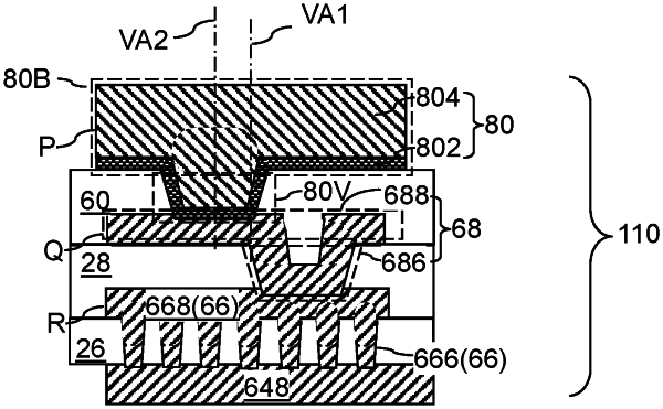
a connection pad-and-via structure located on a first side of the dielectric material layers, wherein the connection pad-and-via structure comprises a connection via portion that vertically extending through a pad-level dielectric material layer and contacting one of the metal interconnect structures and a pad portion contacting a horizontal surface of the pad-level dielectric material layer;
a bump-level dielectric material layer overlying the connection pad-and-via structure; and
a bump structure located on the bump-level dielectric material layer and comprising a bump via portion extending through the bump-level dielectric material layer and contacting the pad portion, wherein an entirety of a bottom surface of the bump via portion is located within an area of a horizontal top surface of the pad portion of the connection pad-and-via structure, wherein a lateral distance between opposing segments of an outer sidewall of the connection via portion is greater than twice a thickness of the pad portion of the connection pad-and-via structure.
|