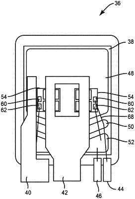
| CPC H01L 24/09 (2013.01) [H01L 24/49 (2013.01); H01L 25/072 (2013.01); H01L 22/14 (2013.01); H01L 22/30 (2013.01); H01L 22/32 (2013.01); H01L 23/49541 (2013.01); H01L 23/49548 (2013.01); H01L 23/49558 (2013.01); H01L 23/49562 (2013.01); H01L 23/49575 (2013.01); H01L 2224/04042 (2013.01); H01L 2924/13055 (2013.01); H01L 2924/13091 (2013.01); H01L 2924/30101 (2013.01)] | 22 Claims |

|
1. A package for power electronics comprising:
a power substrate;
at least two power semiconductor die on the power substrate, each one of the at least two power semiconductor die comprising:
a first power switching pad and a second power switching pad;
a control pad; and
a semiconductor structure between the first power switching pad and the second power switching pad; and
one or more power switching balancing wirebonds coupled between the second power switching pads of each one of the at least two of power semiconductor die.
|