| CPC H01L 24/08 (2013.01) [H01L 21/6835 (2013.01); H01L 23/3114 (2013.01); H01L 23/481 (2013.01); H01L 24/05 (2013.01); H01L 24/11 (2013.01); H01L 24/14 (2013.01); H01L 24/17 (2013.01); H01L 24/19 (2013.01); H01L 24/20 (2013.01); H01L 24/81 (2013.01); H01L 25/0655 (2013.01); H01L 25/0657 (2013.01); H01L 25/105 (2013.01); H01L 25/50 (2013.01); H01L 21/561 (2013.01); H01L 21/568 (2013.01); H01L 23/3128 (2013.01); H01L 23/49816 (2013.01); H01L 23/5383 (2013.01); H01L 23/5389 (2013.01); H01L 24/13 (2013.01); H01L 24/16 (2013.01); H01L 24/29 (2013.01); H01L 24/32 (2013.01); H01L 24/73 (2013.01); H01L 2221/68331 (2013.01); H01L 2221/68345 (2013.01); H01L 2224/02145 (2013.01); H01L 2224/04105 (2013.01); H01L 2224/12105 (2013.01); H01L 2224/13101 (2013.01); H01L 2224/13144 (2013.01); H01L 2224/13147 (2013.01); H01L 2224/13164 (2013.01); H01L 2224/13644 (2013.01); H01L 2224/13655 (2013.01); H01L 2224/13664 (2013.01); H01L 2224/16225 (2013.01); H01L 2224/18 (2013.01); H01L 2224/24137 (2013.01); H01L 2224/2919 (2013.01); H01L 2224/32225 (2013.01); H01L 2224/73204 (2013.01); H01L 2224/73267 (2013.01); H01L 2224/92244 (2013.01); H01L 2225/1058 (2013.01); H01L 2924/1203 (2013.01); H01L 2924/1304 (2013.01); H01L 2924/1432 (2013.01); H01L 2924/1436 (2013.01); H01L 2924/1461 (2013.01); H01L 2924/15192 (2013.01); H01L 2924/15311 (2013.01); H01L 2924/15331 (2013.01); H01L 2924/181 (2013.01); H01L 2924/18161 (2013.01); H01L 2924/19011 (2013.01); H01L 2924/19105 (2013.01); H01L 2924/3511 (2013.01)] | 20 Claims |

|
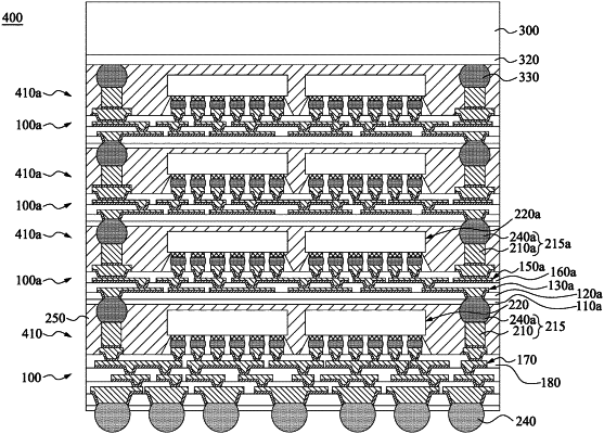
1. A package structure, comprising:
a first dielectric layer;
a first semiconductor device over the first dielectric layer;
a first redistribution line in the first dielectric layer;
a second dielectric layer over the first semiconductor device;
a second semiconductor device over the second dielectric layer;
a second redistribution line in the second dielectric layer;
a conductive through-via over the first dielectric layer, wherein the conductive through-via has a top at a position lower than a top surface of the first semiconductor device;
a conductive ball over the conductive through-via;
a molding material surrounding the first semiconductor device, the conductive through-via, and the conductive ball, wherein a top of the conductive ball is higher than a top surface of the molding material; and
a buffer layer on the top surface of the molding material, wherein the top of the conductive ball is higher than a top of the buffer layer.
|