| CPC H01L 24/08 (2013.01) [H01L 24/05 (2013.01); H01L 24/80 (2013.01); H01L 25/0657 (2013.01); H01L 25/18 (2013.01); H01L 25/50 (2013.01); H10B 41/27 (2023.02); H10B 43/27 (2023.02); H01L 2224/05147 (2013.01); H01L 2224/08145 (2013.01); H01L 2224/80895 (2013.01); H01L 2224/80896 (2013.01); H01L 2924/1431 (2013.01); H01L 2924/14511 (2013.01)] | 20 Claims |

|
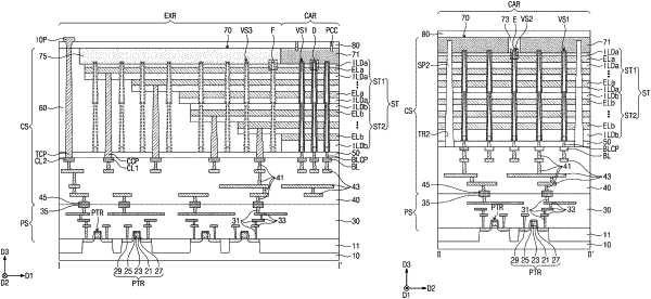
1. A three-dimensional semiconductor memory device, comprising:
a first substrate including a cell array region and a cell array contact region;
a peripheral circuit structure on the first substrate; and
a cell array structure including a stack, first vertical channel structures, second vertical channel structures, and a second substrate,
the stack being on the peripheral circuit structure,
the first vertical channel structures and the second vertical channel structures being on the cell array region and penetrating the stack, and
the second substrate being connected to the first vertical channel structures and the second vertical channel structures,
the stack between the peripheral circuit structure and the second substrate,
the second substrate including a first portion, a second portion, and a third portion,
the first portion being in contact with the first vertical channel structures and doped to have a first conductivity type,
the second portion being in contact with the second vertical channel structures and doped to have a second conductivity type different from the first conductivity type, and
the third portion being on the cell array contact region and doped to have the second conductivity type.
|