| CPC H01L 24/05 (2013.01) [H01L 2224/04042 (2013.01); H01L 2224/05011 (2013.01); H01L 2224/05013 (2013.01); H01L 2224/05014 (2013.01); H01L 2224/05016 (2013.01); H01L 2224/05082 (2013.01); H01L 2224/05088 (2013.01); H01L 2224/05095 (2013.01)] | 18 Claims |
|
1. A semiconductor device comprising:
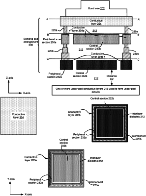
a first layer comprising conductive material, wherein the first layer is a bonding pad layer;
a second layer comprising conductive material underneath the first layer;
one or more interconnects to couple the second layer to the first layer,
wherein the second layer comprises a plurality of discontinuous sections that includes (i) a connected section coupled to the one or more interconnects and (ii) one or more floating sections that are at least in part surrounded by the connected section; and
an under-pad circuit on a substrate underneath the second layer, the under-pad circuit to transmit signals to one or more components external to the semiconductor device through the first layer,
wherein the one or more interconnects comprises an interconnect arranged between a perimeter of the first layer and the connected section of the second layer, such that the interconnect forms a closed loop around the one or more floating sections and such that the interconnect is located between the first layer and the second layer.
|