| CPC H01L 24/05 (2013.01) [H01L 21/56 (2013.01); H01L 24/03 (2013.01); H01L 24/13 (2013.01); H01L 24/45 (2013.01); H01L 2224/0219 (2013.01); H01L 2224/02181 (2013.01); H01L 2224/03019 (2013.01); H01L 2224/0382 (2013.01); H01L 2224/05582 (2013.01); H01L 2224/05624 (2013.01); H01L 2224/05647 (2013.01)] | 23 Claims |
|
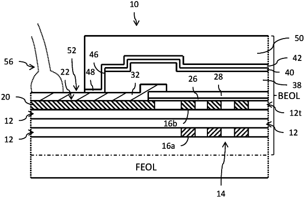
1. An integrated circuit chip, comprising:
a front end of line (FEOL) structure;
a back end of line (BEOL) structure over the FEOL structure;
wherein the BEOL structure includes:
a last metal structure providing a bonding pad;
a passivation structure covering a peripheral region of the last metal structure and including a first opening extending through the passivation structure and exposing an upper surface of the last metal structure;
a conformal nitride layer extending over the passivation structure and in contact with the upper surface of the last metal structure; and
an insulator material layer covering the conformal nitride layer and including a second opening extending through both the insulator material layer and the conformal nitride layer, where a foot portion of the conformal nitride layer on the upper surface of the last metal structure is self-aligned with the second opening.
|