| CPC H01L 23/552 (2013.01) [H01L 21/563 (2013.01)] | 9 Claims |
|
1. A method of making semiconductor device assemblies, comprising:
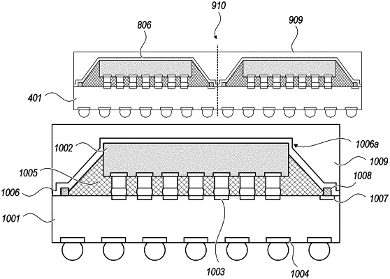
providing a substrate including an upper surface having a plurality of internal contact pads and a plurality of grounding pads and a lower surface having a plurality of external contact pads;
forming a plurality of conductive underfill dams over the upper surface of the substrate, each in electrical contact with a corresponding one of the plurality of grounding pads;
disposing a plurality of semiconductor dies over and in electrical contact with corresponding ones of the plurality of internal contact pads;
dispensing an underfill material at least between each of the plurality of semiconductor dies and the substrate, the underfill material including a fillet between each of the plurality of semiconductor dies and corresponding ones of the plurality of conductive underfill dams wherein the fillet includes a surface extending between and contacting an external sidewall of the plurality of semiconductor dies to intersect and an internal sidewall of the plurality of conductive underfill dams;
forming a plurality of conductive EMI shields, each EMI shield over a corresponding semiconductor die, a corresponding fillet, and a corresponding conductive underfill dam, each EMI shield being conformal with the surface of the corresponding fillet; and
singulating the substrate to separate into a plurality of the semiconductor device assemblies.
|