| CPC H01L 23/5385 (2013.01) [H01L 23/10 (2013.01); H01L 23/5386 (2013.01); H01L 24/04 (2013.01); H01L 24/96 (2013.01)] | 16 Claims |
|
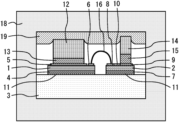
1. A manufacturing method of a semiconductor device comprising:
bonding a semiconductor chip, which includes a main electrode and a control electrode, to a substrate;
bonding a wiring chip, which includes a first electrode, a second electrode and a wiring connecting the first electrode and the second electrode, to the substrate;
bonding a main electrode member to the main electrode via a first bonding material;
bonding a control electrode member to the second electrode via a second bonding material;
bonding the control electrode to the first electrode with a connection member;
putting the semiconductor chip, the substrate, the wiring chip, the main electrode member, the control electrode member and the connection member, which are bonded, into a mold; and
sealing the semiconductor chip, the substrate, the wiring chip, the main electrode member, the control electrode member and the connection member with sealing material by injecting the sealing material into the mold in a state that distal end surfaces of the main electrode member and the control electrode member are pressed against a buffer material provided between the main electrode member and the mold and between the control electrode member and the mold,
wherein the sealing material is not ground.
|