| CPC H01L 23/5384 (2013.01) [H01L 23/3114 (2013.01); H01L 23/5386 (2013.01); H01L 24/14 (2013.01)] | 18 Claims |

|
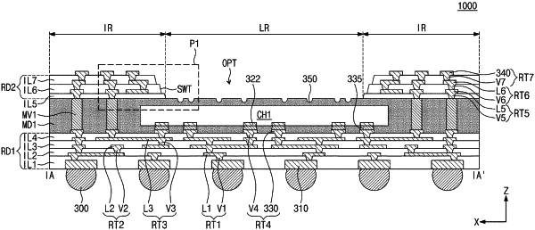
1. A semiconductor package, comprising:
a first semiconductor device on a first redistribution substrate;
a first mold layer that covers the first semiconductor device and the first redistribution substrate; and
a second redistribution substrate on the first mold layer, the second redistribution substrate including:
a first opening that exposes a top surface of the first mold layer, a sidewall of the second redistribution substrate that is exposed to the first opening having a stepwise structure, and
a first redistribution dielectric layer and a second redistribution dielectric layer that are sequentially stacked, sidewalls of the first and second redistribution dielectric layers being offset from each other to form the stepwise structure, and an offset distance between the sidewalls of the first and second redistribution dielectric layers being smaller than a first thickness of the first redistribution dielectric layer and smaller than a second thickness of the second redistribution dielectric layer,
wherein the first mold layer includes grooves on the top surface of the first mold layer, the grooves being spaced apart from a top surface of the first semiconductor device.
|