| CPC H01L 23/49838 (2013.01) [H01L 23/49822 (2013.01); H01L 24/13 (2013.01); H01L 2224/16227 (2013.01)] | 11 Claims |
|
1. A chip scale package (CSP) comprising:
a semiconductor die;
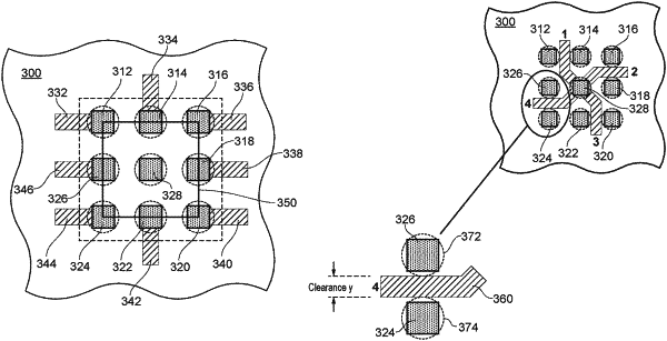
a first set of CSP contact balls or bumps comprising a discontinuous first ring or loop of CSP contact balls or bumps;
a second set of CSP contact balls or bumps, wherein the first and second sets of CSP contact balls or bumps are coupled to the semiconductor die and are positioned within a perimeter of the semiconductor die; and
a channel routing region, the channel routing region being devoid of any CSP contact balls or bumps;
wherein the first and second sets of CSP contact balls or bumps are configured for directly mounting the CSP on, and electrically coupling the CSP to, a substrate of a host device incorporating the CSP, and the CSP is approximately the same size as the semiconductor die; and
wherein the channel routing region is provided, at least in part, by a discontinuity in the first ring or loop.
|