| CPC H01L 23/49838 (2013.01) [H01L 21/4857 (2013.01); H01L 23/3128 (2013.01); H01L 23/49822 (2013.01); H01L 23/562 (2013.01)] | 17 Claims |
|
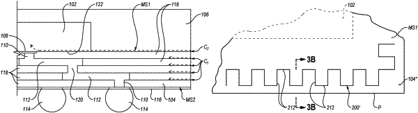
1. A redistribution layer (RDL) structure, comprising:
at least one level of conductive traces between adjacent levels of low-k dielectric material; and
a reinforcement structure comprising first beams extending parallel to and inward of a periphery of the RDL structure, each of the first beams having a first length, and second beams extending perpendicular to the periphery, each of the second beams having a second length, the second length equal to, or greater than, the first length, each of the second beams connected to two of the first beams, the reinforcement structure comprised of a conductive material, the reinforcement structure electrically isolated from the at least one level of conductive traces and extending between a first major surface and a second major surface of the RDL structure;
wherein the first beams and the second beams define a square-wave pattern when viewed from the first major surface.
|