| CPC H01L 23/49827 (2013.01) [H01L 21/486 (2013.01); H01L 21/4853 (2013.01); H01L 23/49811 (2013.01); H01L 23/49894 (2013.01); H01L 25/0655 (2013.01); H01L 25/18 (2013.01); H01L 23/147 (2013.01); H01L 23/3675 (2013.01); H01L 24/73 (2013.01); H01L 2224/73204 (2013.01)] | 19 Claims |

|
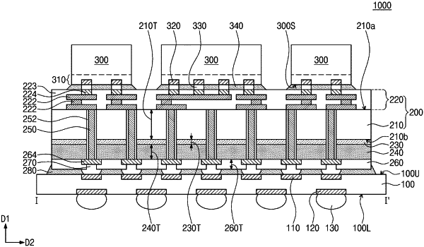
1. A semiconductor package comprising:
an upper substrate having a first surface and a second surface which are opposite to each other;
a semiconductor chip on the first surface of the upper substrate;
a buffer layer on the second surface of the upper substrate;
a mold layer between the second surface of the upper substrate and the buffer layer;
a plurality of through-electrodes penetrating the upper substrate and the mold layer;
an interconnection layer between the first surface of the upper substrate and the semiconductor chip and configured to electrically connect the semiconductor chip to the plurality of through-electrodes, wherein the interconnection layer contacts the plurality of through-electrodes;
a plurality of bumps disposed on the buffer layer, spaced apart from the mold layer, and electrically connected to the plurality of through-electrodes, wherein the mold layer includes an insulating material of which a coefficient of thermal expansion is greater than that of the upper substrate; and
an insulating layer between the second surface of the upper substrate and the mold layer,
wherein each of the plurality of through-electrodes further penetrates the insulating layer, and
wherein a thickness in a first direction of the mold layer is less than a thickness in the first direction of the upper substrate, and the first direction is perpendicular to the first surface of the upper substrate.
|