| CPC H01L 23/49811 (2013.01) [H01L 21/481 (2013.01); H01L 21/4853 (2013.01); H01L 23/49822 (2013.01); H01L 23/49838 (2013.01); H01L 24/08 (2013.01); H01L 24/16 (2013.01); H01L 2224/08225 (2013.01); H01L 2224/16227 (2013.01)] | 14 Claims |

|
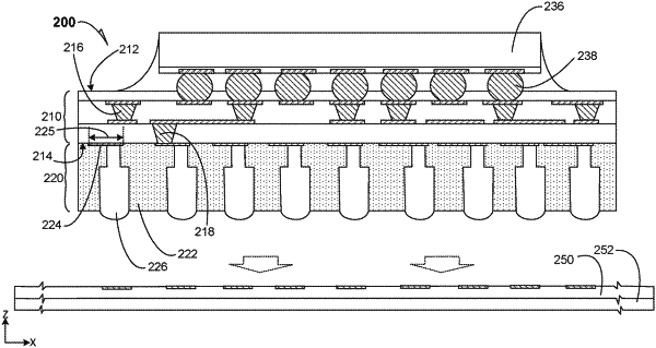
1. A method of forming an encapsulated interconnect, the method comprising:
forming an encapsulation material on a land side of a semiconductor package substrate to contact a trace on the land side, the encapsulation material having an encapsulation height;
forming a via in the encapsulation material;
depositing a vertical interconnect in the via at a terminal end of the trace, the vertical interconnect having a portion that extends beyond the encapsulation height, the vertical interconnect having a stepped right-cylindrical cross-sectional area;
drilling a first right-cylindrical via in the encapsulation material to expose the trace at a terminal end, the first right-cylindrical via having a first characteristic dimension;
drilling a second right-cylindrical via in the encapsulation material after drilling the first right-cylindrical via, the second right-cylindrical having a second characteristic dimension that is larger than the first characteristic dimension wherein the first characteristic dimension is a height of the first right-cylindrical via and the second characteristic dimension is a height of the second right-cylindrical via; and
filling the via by a process selected from electroplating and solder printing.
|