| CPC H01L 23/481 (2013.01) [H01L 21/76841 (2013.01); H01L 21/76898 (2013.01)] | 10 Claims |

|
1. A manufacturing method of a through silicon via structure for three-dimensional integrated circuit packaging, comprising steps of:
lifting off a silicon wafer by implanting hydrogen ions into the silicon wafer to obtain a substrate for making a through silicon via;
performing double-sided plasma etching on the substrate to form a through silicon via penetrating the substrate;
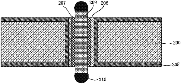
depositing sequentially an insulating medium, a copper diffusion barrier layer, and a seed layer on a sidewall of the through silicon via and upper and lower surfaces of the substrate, and removing parts of the copper diffusion barrier layer and the seed layer by photolithography and etching processes, leaving only parts of the copper diffusion barrier layer and the seed layer on the sidewall of the through silicon via;
forming a sacrificial layer on upper and lower surfaces of the resulting structure, completely filling the through silicon via with conductive metal material, and then removing the sacrificial layer, upper and lower surfaces of the conductive metal material respectively protruding from upper and lower surfaces of the insulating medium; and
forming contact pads on surfaces of the conductive metal material;
wherein the conductive metal material is in direct contact with the seed layer, and the conductive metal material is not in direct contact with the sacrificial layer;
wherein the insulating medium disposed on the sidewall of the through silicon via is covered by the copper diffusion barrier layer, the upper and lower surfaces of the insulating medium are not covered by the copper diffusion barrier layer, and the copper diffusion barrier layer disposed on the sidewall of the through silicon via is covered by the seed layer.
|