| CPC H01L 23/10 (2013.01) [H01L 23/049 (2013.01); H01L 23/3735 (2013.01); H01L 23/24 (2013.01); H01L 24/73 (2013.01); H02P 27/06 (2013.01)] | 7 Claims |
|
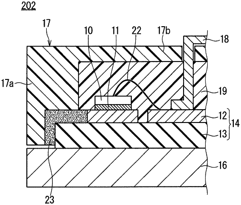
1. A semiconductor device comprising:
a base plate;
an insulating substrate including a ceramic plate and a circuit pattern, the ceramic plate being integrally bonded to an upper surface of the base plate with no solder layer therebetween, the circuit pattern being disposed on an upper surface of the ceramic plate;
a semiconductor element mounted on an upper surface of the circuit pattern;
a case surrounding the insulating substrate and the semiconductor element over the base plate;
an adhesive to adhere a lower portion of the case to an outer peripheral portion of the ceramic plate; and
a sealant to seal an interior of the case, wherein
the adhesive is in contact with an outer peripheral end of the ceramic plate to an outer peripheral end of the circuit pattern.
|