| CPC H01L 23/053 (2013.01) [H01L 23/14 (2013.01); H01L 23/3114 (2013.01); H01L 23/367 (2013.01); H01L 23/49838 (2013.01)] | 11 Claims |
|
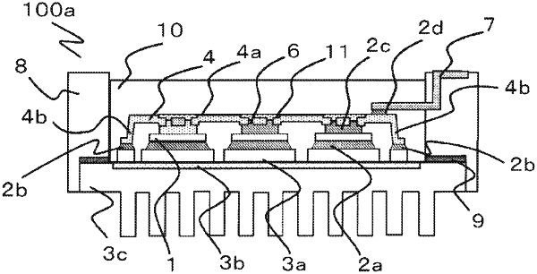
1. A power semiconductor device comprising:
a semiconductor element;
a circuit pattern mounted with the semiconductor element;
an insulating layer mounted with the circuit pattern;
a heat radiation fin mounted with the insulating layer;
a case bonded to a peripheral edge of the heat radiation fin and surrounding the semiconductor element, the circuit pattern, and the insulating layer;
a sealing resin sealed in a region surrounded by the insulating layer, the circuit pattern, and the case;
an internal electrode bonded to the semiconductor element and the circuit pattern, including a flat plate-shaped portion, and including a pair of support portions; and
an external electrode bonded to the internal electrode and integrally molded with the case.
|
|
10. A method for manufacturing a power semiconductor device, the method comprising the steps of:
bonding a semiconductor element to a circuit pattern mounted on a heat radiation fin with interposition of an insulating layer;
bonding the semiconductor element to an internal electrode, and bonding a support portion of the internal electrode to the circuit pattern;
bonding the heat radiation fin to a case;
bonding the internal electrode to an external electrode integrally molded with the case;
wire-bonding and connecting by wiring the semiconductor element to a control terminal integrally molded with the case with a metal wire; and
sealing with resin a region surrounded by the insulating layer, the circuit pattern, and the case.
|