| CPC H01L 21/7806 (2013.01) [H01L 21/0254 (2013.01); H01L 21/02447 (2013.01); H01L 21/02529 (2013.01); H01L 21/76254 (2013.01); H01L 29/045 (2013.01); H01L 29/1608 (2013.01); H01L 29/2003 (2013.01); H01L 29/267 (2013.01)] | 20 Claims |

|
1. A method of manufacturing a semiconductor substrate comprising:
epitaxially growing a buffer layer and a silicon carbide layer on a silicon surface of an N-type silicon carbide substrate, wherein the silicon carbide layer is high-resistivity silicon carbide or N-type silicon carbide (N—SiC);
epitaxially growing a gallium nitride epitaxial layer on the silicon carbide layer to obtain a semiconductor structure composed of the buffer layer, the silicon carbide layer, and the gallium nitride epitaxial layer;
using a laser to form a damaged layer in the semiconductor structure after epitaxially growing the gallium nitride epitaxial layer;
bonding a chip carrier on a surface of the gallium nitride epitaxial layer; and
separating the N-type silicon carbide substrate and the semiconductor structure at where the damaged layer is disposed.
|
|
13. A method of manufacturing a semiconductor substrate, comprising:
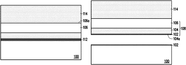
using ion implantation to form a damaged layer on a silicon surface of an N-type silicon carbide substrate;
epitaxially growing a buffer layer and a silicon carbide layer on the silicon surface of the N-type silicon carbide substrate after the damaged layer is formed, wherein the silicon carbide layer is high-resistivity silicon carbide or N-type silicon carbide (N—SiC);
epitaxially growing a gallium nitride epitaxial layer on the silicon carbide layer to obtain a semiconductor structure composed of the buffer layer, the silicon carbide layer, and the gallium nitride epitaxial layer;
bonding a chip carrier on a surface of the gallium nitride epitaxial layer; and
separating the N-type silicon carbide substrate and the semiconductor structure at where the damaged layer is disposed.
|