| CPC H01L 21/78 (2013.01) [H01L 21/56 (2013.01); H01L 22/14 (2013.01); H01L 22/32 (2013.01); H01L 23/10 (2013.01); H01L 23/3171 (2013.01)] | 19 Claims |
|
1. A method for forming a semiconductor die, the method comprising:
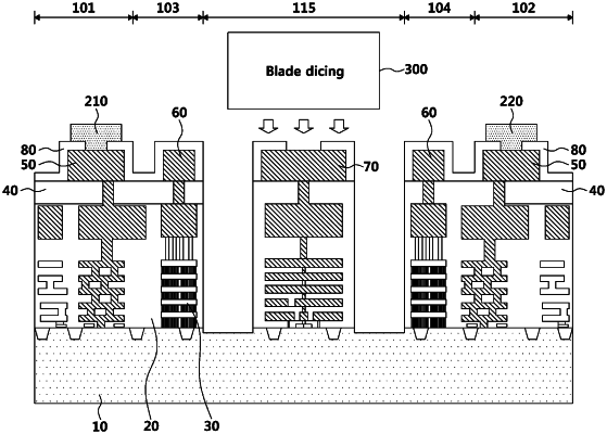
forming an interlayer dielectric layer on a substrate having a semiconductor die region, a seal-ring region, and a scribe line region;
forming a metal pad and a test pad on the interlayer dielectric layer;
forming a passivation dielectric layer on the interlayer dielectric layer, the metal pad, and the test pad;
first etching the passivation dielectric layer and the interlayer dielectric layer existing between the seal-ring region and the scribe line region to a predetermined depth using a plasma etching process;
second etching the passivation dielectric layer to expose the metal pad and the test pad;
forming a bump on the metal pad; and
dicing the substrate while removing the scribe line region by mechanical sawing.
|